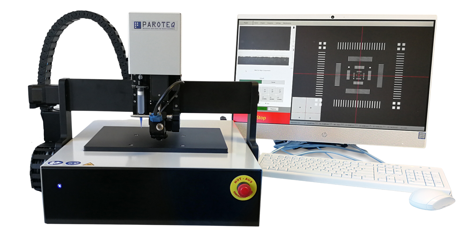
H-System GA Die/Flip Chip Bonder
The H-System GA is a versatile placement system featuring an overhead gantry configuration with integrated beam splitter optics. This configuration ensures a maximum working area with a minimal footprint as a benchtop unit. The integrated beam splitter optics for real-time image overlay enable the operator to align components and substrates intuitively and precisely. The force-controlled Z-axis accommodates varying bond heights and ensures a reproducible bonding process. A second Z-axis can be used without tool changes for loading or unloading single or connected components, as well as for dispensing, dipping, or stamping. Integrated heating plates, heated holders, or dispensers support the respective bonding process. The H-System GA supports all current and future bonding technologies and applications in the field of microsystems engineering. The H-System GA runs on paroPro, a proprietary software interface developed by Paroteq that enables intuitive and flexible control of high-precision micro-assembly processes.
Applications
- Die Bonding
- Flip Chip Bonding
- CoS (chip on Submount)
- MEMS / MOEMS assembly
- Sensor assembly
- Assembly of optical components (photo diodes, laser diodes)
- Assembly of lenses and lens arrays
- Laser bar bonding
- Assembly of mechanical components
- Sorting of components
- Assembly of medical parts
Options
- HMTPA (high magnified two point alignment)
- Different light sources
- Dispensing / stamping
- UV-curing
- Heated pick up tools
- Heating plates with and w/o vacuum structure
- Coplanarity tools
- Process gas chamber
- Process gas suction
- Support plate with vacuum
- Input-/output station with or without vacuum
- Inspection camera
Technologies
- Thermo-compression bonding (eutectic bonding Au/Sn, Au/Au bonding)
- Ultrasonic - or thermosonic bonding
- Adhesive bonding
- Dispensing
- Dipping
- Stamping
- UV curing
Technical Specifications
- Overhead gantry arrangement
- Beam splitter optics
- Fully programmable bond process
- Height adjustable bond stage
- Bond force: 10 - 500cN
- Positioning accuracy: 5 micron
- Maximum component size: 25 mm x 25 mm
- Maximum substrate size: 300 mm x 300 mm
- Working area: 300 mm x 240 mm
- Foot print: 600 mm x 600 mm x 420 (LxWxH)